Transistors, often hailed as the building blocks of modern electronics, play a pivotal role in amplifying or switching electrical signals.
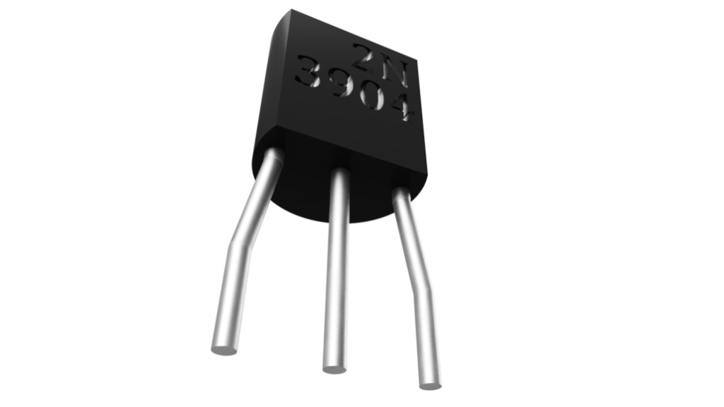
In this discussion, we will dive deeply into bipolar junction transistors (BJTs), particularly focusing on their two types: NPN and PNP. BJTs are widely used in analog and digital circuits for amplification, switching, and signal modulation tasks. We’ll explore their structure, functionality, and application and how to use them effectively in circuits.
The Basic Structure of BJTs
A Bipolar Junction Transistor (BJT) is a type of transistor that uses both electron and hole charge carriers (hence the term “bipolar”) to control the flow of current. It is a three-terminal device composed of semiconductor materials, designed to amplify or switch electrical signals in various circuits.
The three terminals of a BJT are:
- Emitter (E): This terminal is heavily doped to emit charge carriers (electrons in NPN or holes in PNP).
- Base (B): A thin, lightly doped layer that controls the transistor’s operation by allowing or restricting the flow of carriers.
- Collector (C): The region where the charge carriers are collected, driving current from the emitter to the collector when the transistor is turned on.
Types of BJTs
There are two types of BJTs, based on the arrangement of their semiconductor layers.
Modes of Operation
- Active Mode: The transistor operates as an amplifier. The base-emitter junction is forward-biased, and the collector-base junction is reverse-biased.
- Saturation Mode: Both junctions are forward-biased. The transistor acts as a closed switch, allowing maximum current to flow.
- Cutoff Mode: Both junctions are reverse-biased. The transistor acts as an open switch and no current flows.
NPN vs. PNP: Key Differences in Structure
The main distinction between NPN and PNP transistors lies in the arrangement of semiconductor layers and, consequently, the direction of current flow through the device. To understand how these semiconductor materials work, check out our article on how a diode works.
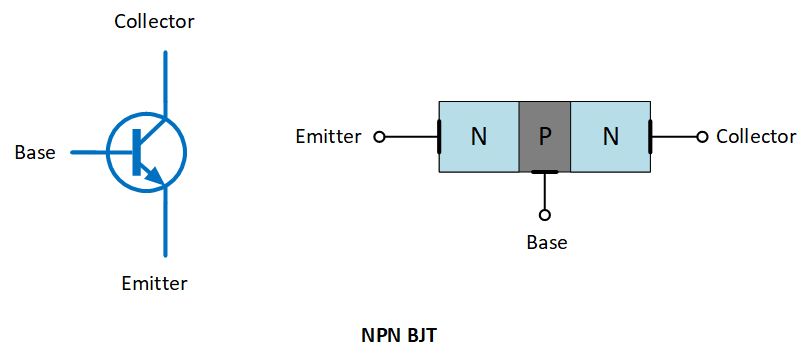
NPN Transistor Diagram
The structure of an NPN transistor consists of a layer of P-type semiconductor (base) sandwiched between two N-type semiconductors (emitter and collector).
NPN Transistor Operation
Current Flow:
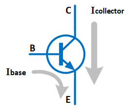
In an NPN transistor, current flows from the collector to the emitter (C to E) when the base is supplied with a small positive voltage.
Biasing:
- The base-emitter junction must be forward-biased. This means the base is more positive than the emitter (typically by ~0.7V for silicon transistors).
- The collector-base junction is reverse-biased (the collector is more positive than the base).
When the base-emitter junction is forward-biased, electrons move from the emitter into the base. Some electrons combine with holes in the base, but most are pulled into the collector because of the reverse bias between the collector and base.
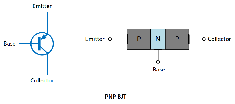
PNP Transistor Diagram
PNP transistor has the opposite structure, with an N-type (base), sandwiched between two P-type semiconductors (emitter and collector).
PNP Transistor Operation
Current Flow:
In a PNP transistor, current flows from the emitter to the collector (E to C) when the base is supplied with a small negative voltage.
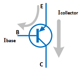
Biasing:
- The base-emitter junction must be forward-biased, with the base being more negative than the emitter.
- The collector-base junction is reverse-biased (the collector is more negative than the base).
In this configuration, holes move from the emitter into the base. Some recombine in the base, but most continue to the collector.
Note: The PNP operation is essentially the inverse of the NPN transistor, but the principle of control remains the same: a small base current controls a larger emitter-collector current.
Transistors as Amplifiers
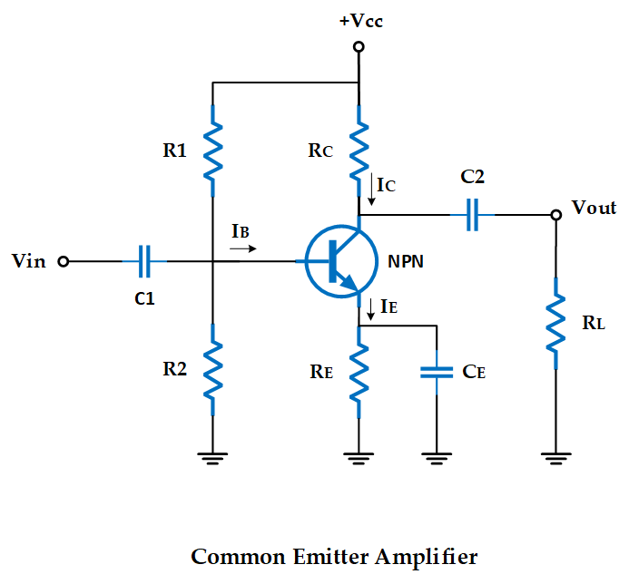
A transistor works as an effective amplifier by controlling the flow of a large current using a smaller input signal. The transistor essentially boosts the amplitude of the input signal, making it larger at the output.
For example, the figure below shows a common-emitter amplifier using an NPN transistor. It is the most popular configuration for using NPN transistors due to their simplicity and ability to provide high gain. In this setup, the emitter is grounded (or connected to a common reference point), the input signal is applied to the base, and the output signal is taken from the collector.
Push-Pull Amplifiers
Both NPN and PNP transistors are often used together in push-pull amplifier configurations, where they alternately conduct, allowing efficient amplification with minimal power loss. This is commonly found in audio amplifiers, where complementary NPN and PNP transistors help to reduce distortion.
The Key Concept of Gain (Current Amplification)
As discussed earlier, NPN and PNP transistors can amplify small input signals. The ratio of the collector current to the base current is known as the current gain (β or hFE).
\[β= \frac{I_C}{I_B}\]
For both types of transistors, typical β values range from 20 to 100, depending on the transistor model and operating conditions.
Switching Applications
The fundamental principles of operation are the same; basically, PNP transistors can perform the same functions as NPN transistors. The only difference is they are configured differently in circuits due to their complementary polarities.
NPN Transistor as a Switch
NPN transistors are more commonly used in switching circuits, where they control the flow of current through loads that are connected to a positive supply. Here’s a typical NPN switch circuit.
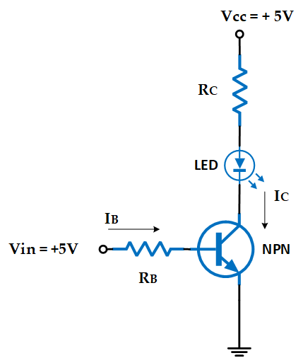
- The collector is connected to a load, an LED in this example, and a positive voltage source.
- The emitter is grounded.
In the circuit, a small base current (IB) activates the transistor. This allows a larger current (IC) to flow from the collector to the emitter. This current flow then powers the LED, illuminating it.
This configuration is known as a low-side switch because the load is connected to the positive voltage, and the transistor switches the ground connection.
PNP as a Switch
PNP transistors, by contrast, are used in high-side switch configurations, where the load is connected to the ground, and the transistor switches the positive voltage. The figure below shows a typical PNP switch circuit.
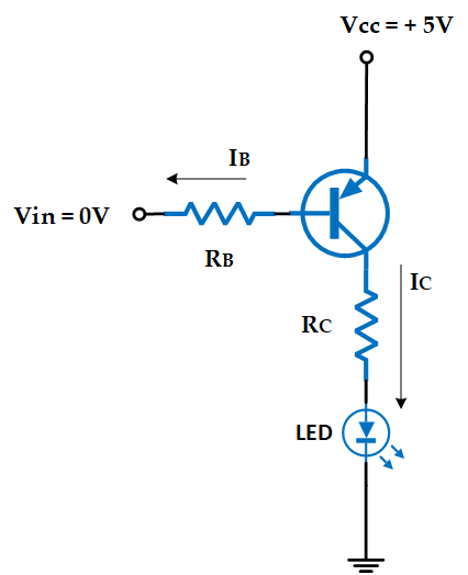
- The emitter is connected to a positive voltage source (Vcc).
- The collector is connected to the LED, which is grounded.
The same principle applies to PNP transistors. But this time, a small current (IB) flowing out of the base turns on the transistor. This allows current (IC) to flow from the emitter to the collector, powering the LED.
ⓘ Note
Please note that to make both circuits function properly, you have to calculate the correct resistor values for RC and RB.
Key Specifications and Differences
While NPN and PNP transistors have the same working principle, there are still a few notable points that you need to consider.
- Input Signal Polarity: NPN transistors require a positive base voltage to operate, while PNP transistors need a negative base voltage.
- Common Grounding: NPN transistors work well with ground-referenced circuits since they “sink” current. On the other hand, PNP transistors source current, so they’re better for circuits where positive voltage references are used.
- Speed: NPN transistors generally offer faster switching speeds than PNP types due to electrons’ higher mobility than holes. This makes NPN transistors preferable in high-speed applications like digital logic circuits.
- Power Dissipation: Both types of transistors can dissipate heat during operation, but NPN transistors are more efficient in many designs due to their faster electron flow.
Practical Transistor Models
- 2N2222: A popular general-purpose NPN transistor, known for its robustness and switching capabilities.
- 2N3904: Another common NPN transistor, widely used in switching and amplification circuits.
- 2N2907: A common PNP transistor used in switching applications.
- 2N3906: The PNP counterpart to the 2N3904, commonly found in general-purpose applications.
Creator and Editor at AnitoCircuits.com based in Toronto