Almost every electronic device you own runs on a regulated DC voltage. Your phone, laptop, Arduino, LED strip, and solar charge controller — all of them need power at a specific voltage, regardless of what the input source provides. The components that make this happen are called DC-to-DC converters, and the three most important topologies are the buck, the boost, and the buck-boost.
This article breaks down all three converters from the ground up: what they do, how they work step-by-step, the key formulas, real-world applications, and accurate circuit schematics for each topology.
Switching Converter
The old-school way to reduce a voltage was to use a linear regulator, a device that essentially burns off the excess voltage as heat. For instance, at 1A of load current, stepping down from 12V to 5V means 7 watts of heat. That’s over half of your input power being wasted.
Switching converters is fundamentally different. Instead of throwing away energy, they rapidly switch power on and off and use inductors and capacitors to store and release energy at a different voltage. A well-designed switching converter achieves 90–95% efficiency, compared to as low as 40% for a linear regulator in the same situation.
All three switching topologies share the same core components: a switch (MOSFET), an inductor, a diode (or synchronous switch), and an output capacitor. The arrangement and switching strategy determine whether the converter bucks, boosts, or both.
Buck Converter (Step-Down)
The buck converter is the most common DC-to-DC topology in existence. Its job is simple: take a higher input voltage and deliver a lower, regulated output voltage.
You’ll find a buck converter on virtually every microcontroller board, inside USB chargers, and on any PCB that runs chips at 3.3V or 1.8V from a 5V or 12V supply.
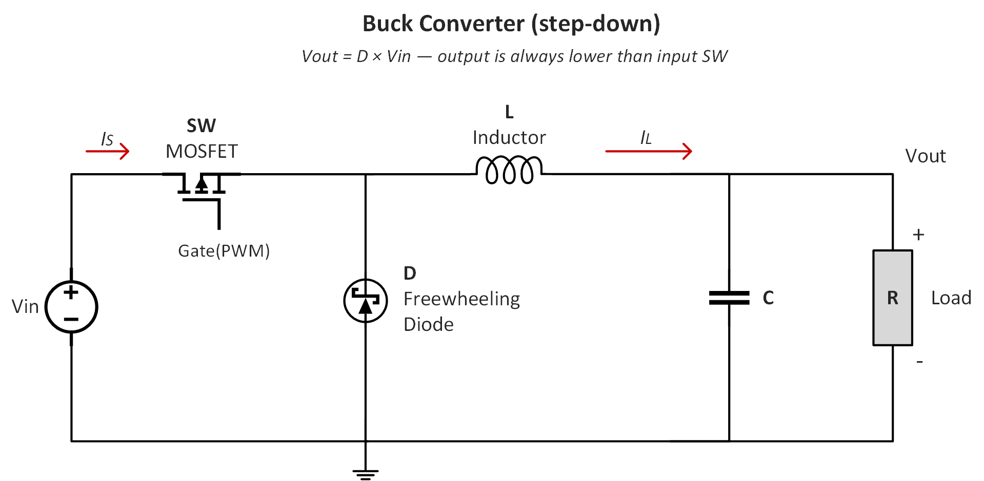
How It Works
Phase 1 — Switch ON
When the MOSFET closes, the input voltage is connected directly to the inductor. Current ramps up gradually through the inductor (which resists sudden changes), storing energy in its magnetic field. The load is supplied directly during this phase.
Phase 2 — Switch OFF
When the MOSFET opens, the inductor maintains current flow by generating a voltage that forward-biases the freewheeling diode. Current continues circulating through the load via the diode, while the inductor releases its stored energy. The output capacitor smooths the ripple.
Buck Converter Output Voltage:
\[ Vout= V\times V_{in} \]D = duty cycle (0 to 1). Example: D = 0.42, Vin = 12V → Vout = 5V
Real-World Applications
- Microcontroller boards: stepping 5V or 12V down to 3.3V or 1.8V for logic circuits
- CPU power delivery: modern processors run sub-1V; a buck steps down the motherboard’s 12V rail
- USB power banks: convert internal 3.7V Li-ion up to 5V output — wait, that’s boost! The internal management IC uses a buck to charge the cell from USB
- Solar MPPT controllers: buck topology charges 12V batteries from higher-voltage panel strings
- LED drivers: constant-current buck converters drive LED strings efficiently
ⓘ Quick Tip!
ICs labelled LM2596, MP2307, XL4016, or TPS54360 are buck controller chips. They’re extremely common in DIY power supply modules.
Boost Converter (Step-Up)
The boost converter takes a lower input voltage and produces a higher output. This seems almost magical. How can you get more voltage out than you put in? The answer is energy conservation: the converter trades lower current for higher voltage, keeping power (P = V × I) constant minus losses.
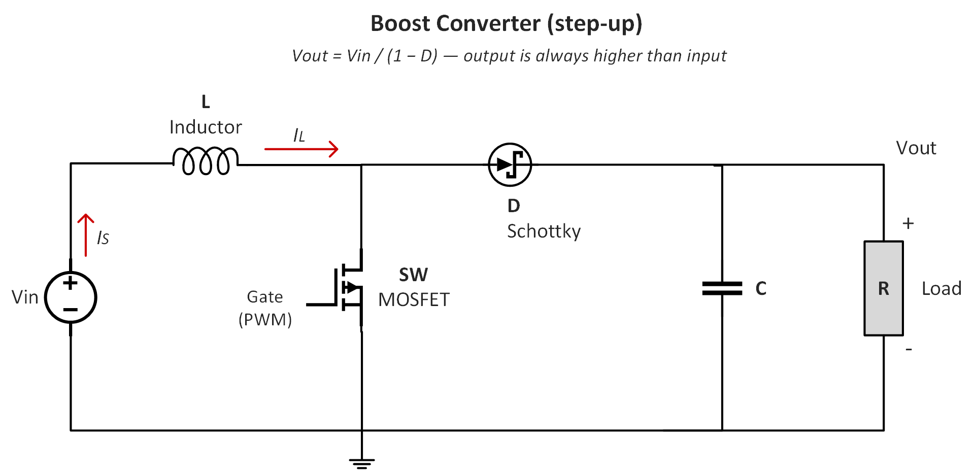
How It Works
Phase 1 — Switch ON
The MOSFET creates a short to GND on one end of the inductor. Current flows from the input through the inductor to ground, ramping up and storing energy. The output diode is reverse-biased — the capacitor supplies the load alone.
Phase 2 — Switch OFF
The MOSFET opens; the inductor’s collapsing field generates a voltage spike. This spike adds to the input voltage (inductor acts as a series voltage source), forward-biasing the diode and pushing a boosted voltage into the output capacitor and load.
Boost Converter Output Voltage:
\[ Vout= \frac {V_{in}}{(1-D)} \]D = duty cycle. Example: D = 0.6, Vin = 5V → Vout = 12.5V. As D → 1, Vout → ∞ (limited by component losses in practice)
Real-World Applications
- LED drivers: white/blue LEDs need 3.2–3.6V forward voltage; a boost can drive them from a 1.5V AA cell
- Camera flash circuits: boost battery voltage to 300V+ to charge the flash capacitor almost instantly
- UPS and battery backup: boost a dropping battery to maintain a stable output voltage
- RF power amplifiers: boost 3.3V logic rail to 5V or higher for RF output stages
- Power Factor Correction (PFC): The PFC stage in almost every quality AC-DC supply is a boost converter shaping the input current waveform
Buck-Boost Converter
The buck-boost is the most flexible of the three. It can produce an output that is either higher or lower than the input, making it essential for applications where the input voltage varies and may cross above or below the required output.
The classic example: a lithium-ion battery starts at 4.2V when fully charged and discharges to 3.0V. If you need a stable 3.3V output, the battery starts above the target (buck needed) and ends below it (boost needed). A buck-boost handles the entire discharge curve seamlessly.
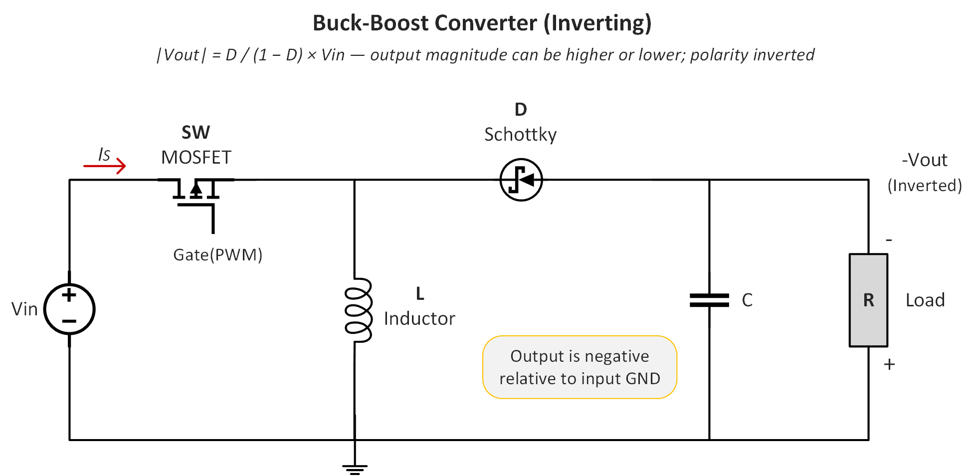
Two Main Topologies
1. Inverting Buck-Boost (Classic, Single-Switch)
The simplest buck-boost uses one switch, one inductor, one diode, and one capacitor. Similar parts count to a buck or boost but are arranged differently. The trade-off is that the output voltage is inverted (negative polarity) relative to the input ground.
Minus sign (not shown) indicates polarity inversion. D = 0.5 → |Vout| = Vin. D < 0.5 → buck mode. D > 0.5 → boost mode.
2. Non-Inverting Buck-Boost (4-Switch)
To avoid polarity inversion, a 4-switch topology is used. More complex and slightly less efficient, but outputs positive voltage whether bucking or boosting. This is used in most modern smartphones and IoT devices.
The 4-switch buck-boost dynamically transitions between pure buck, pure boost, and combined mode as the input voltage varies relative to Vout. The transition region near Vin ≈ Vout requires careful control to avoid output glitches.
Real-World Applications
- Smartphones and tablets: stable voltage regulation across the full Li-ion discharge from 4.2V to 3.0V
- IoT and wireless sensors: stable 3.3V from a coin cell (3.0V to 1.8V over its life)
- Automotive electronics: the car 12V battery swings from 8V during cranking to 14.4V during charging — a buck-boost handles the full range
- Solar MPPT (wide range): input from panels varies widely with sunlight; a buck-boost maintains a stable charge voltage regardless
Gate Signal and Inductor Current Waveforms
Understanding how the gate signal and inductor current behave is fundamental to designing and troubleshooting switching converters. The same basic waveform shapes appear in all three topologies.
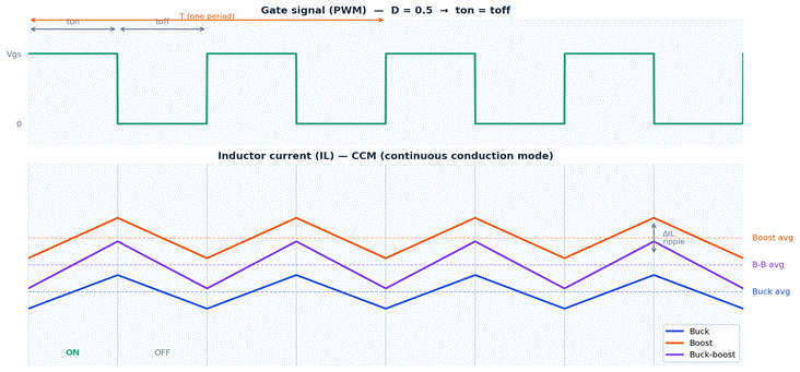
In Continuous Conduction Mode (CCM), the inductor current never reaches zero between switching cycles. This gives lower ripple and better regulation but requires a larger inductor. At light loads, the converter transitions to Discontinuous Conduction Mode (DCM), where current touches zero each cycle — changing the gain equation but potentially improving light-load efficiency.
Side-by-Side Comparison
A quick reference across the most important parameters for all three topologies:
| Feature | Buck | Boost | Buck-Boost |
| Output vs Input | Lower (step-down) | Higher (step-up) | Higher OR Lower |
| Output Polarity | Same as input | Same as input | Inverted (basic) |
| Efficiency | High (~90–95%) | High (~85–92%) | Moderate (~80–88%) |
| Circuit Complexity | Low | Low | Higher |
| Duty Cycle (D) | Vout = D × Vin | Vout = Vin/(1−D) | |Vout| = D/(1−D) × Vin |
| Typical Use | CPU power rails | LED drivers, UPS | Battery systems, IoT |
As a rule of thumb, use the simplest topology that meets your requirements. If your input is always higher than your output, a buck is simpler, cheaper, and more efficient than a buck-boost. Only reach for the buck-boost when you genuinely need the voltage flexibility.
Choosing Key Components
Inductor
- Inductance (μH): higher inductance = lower current ripple but larger size. Typical values: 1μH–470μH depending on frequency and power.
- Saturation current: must exceed peak inductor current — saturation causes inductance collapse and potentially destructive current spikes.
MOSFET Switch
- Vds rating: must exceed peak switch voltage with 20–50% margin for transients
- Rds(on): on-resistance causes conduction losses — lower is better
- Gate charge (Qg): lower gate charge = faster switching = lower switching losses
Output Capacitor
Low-ESR capacitors are critical. High ESR converts ripple current into output voltage ripple. Ceramic (MLCC) capacitors have the lowest ESR; electrolytics offer high capacitance at lower cost.
Diode
Use Schottky diodes for their lower forward voltage drop (0.2–0.4V vs 0.6–0.7V) and faster switching speed. Many modern ICs replace the diode with a synchronous MOSFET (synchronous rectification) to further reduce losses.
Popular Converter ICs for Hobbyists
Buck ICs
- LM2596: classic, easy to use, 3A, adjustable or fixed — very popular for DIY power supplies
- MP1584 / MP2307: small, high-frequency — found on cheap buck modules
- TPS54360: professional-grade, 60V input, excellent TI datasheet with design calculator
Boost ICs
- MT3608 / SDB628: very popular in cheap boost modules, 2A, up to 28V output
- XL6009: higher efficiency than MT3608, 4A output
- TPS61023: Texas Instruments 1A boost — excellent for single-cell battery-powered IoT
Buck-Boost ICs
- TPS63000: non-inverting buck-boost, perfect for 3.3V from Li-ion — widely used in IoT devices
- LTC3780: high-efficiency 4-switch buck-boost, popular in advanced DIY supplies
- MAX17222: nano-power buck-boost for ultra-low-power sensor applications
ⓘ Tip!
Buy a ready-made module rather than designing from scratch. A less than $2 MT3608 boost module from ebay.com or LM2596 buck module from amazon.com lets you prototype immediately. Once you understand the topology behaviour, design your own PCB with the IC directly.
Creator and Editor at AnitoCircuits.com based in Toronto