Design Goals
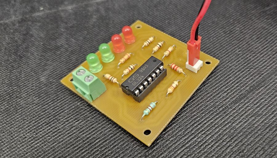
The diagram provided shows an LED bar graph meter circuit that utilizes operational amplifiers. The objective of this project is to design the PCB board for the circuit using EAGLE software and physically construct it. The process involves computations of values, circuit simulation on ORCAD and breadboard, and confirming the circuit’s operational principle.
| Parameters | Value | |
| Supply Voltage, Vcc | 9V | |
| Vin | Vin (min) | Vin (max) |
| 0V | 6V | |
| Vout | Vout (min) | Vout (max) |
| 0.1V | 4.9V | |
| Reference Voltages: | ||
| Vref1 | 5.31V | |
| Vref2 | 3.825V | |
| Vref3 | 2.835V | |
| Vref4 | 1.08V | |
Design Description
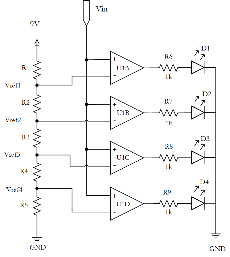
The opamps are configured as comparators. Each is designed to compare the input voltage (Vin), connected to its non-inverting input, with the reference voltage applied to its inverting input terminal. Whenever Vin is equal to or greater than the reference voltage connected to a particular opamp, the corresponding LED lights up. This provides a clear visual representation of the input voltage level.
Featured Op amp
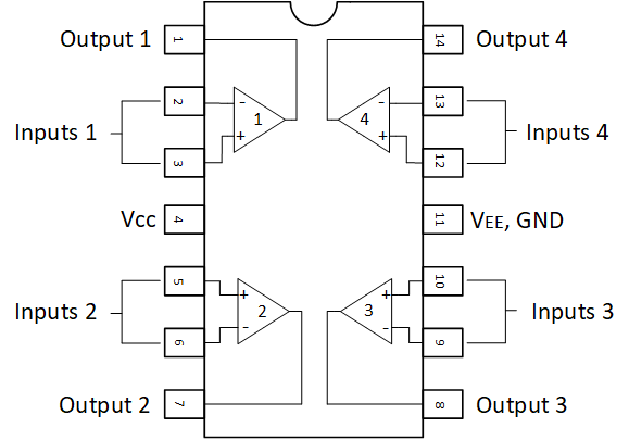
The circuit utilizes the LM324 IC, comprising four self-contained operational amplifiers. The LM324 is a cost-effective option for quad-operational amplifiers and is capable of functioning with supply voltages ranging from 3.0 V to 32 V.
| LM324 | |
| Vcc | 3V to 32V, 1.5mA |
| Output Current | 40mA |
| VIDR | ±32V |
| VICR | −0.3V to 32V |
| Number of Circuits | 4 |
| Datasheet: https://www.onsemi.com/pdf/datasheet/lm324-d.pdf | |
LM324 Pin Outs Diagram
Alternate Quad Operational amplifiers: TL074, TL084 and LM2902
Design Calculations
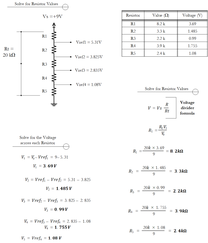
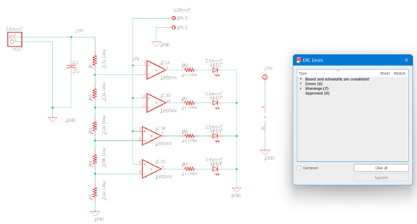
The four distinct reference voltages are defined by the supply voltage and five resistors connected in series, forming a voltage divider circuit, as shown in the figure below. Now, this step is aimed to determine each of these resistances.
- To get the resistor values, the voltage across each resistor should be calculated first.
- Then each resistance can be calculated using the voltage divider formula.
Bias Point Simulation Result
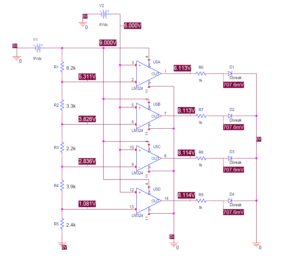
Note that this simulation is only intended to verify the values that were calculated earlier. This does not show the expected behavior of the circuit. To get the actual transient response, it’s recommended to use software that is more capable of doing it. This project only attempts to determine DC bias points and will rather focus on the actual circuit simulation using a breadboard.
Circuit Prototype (Breadboarding)
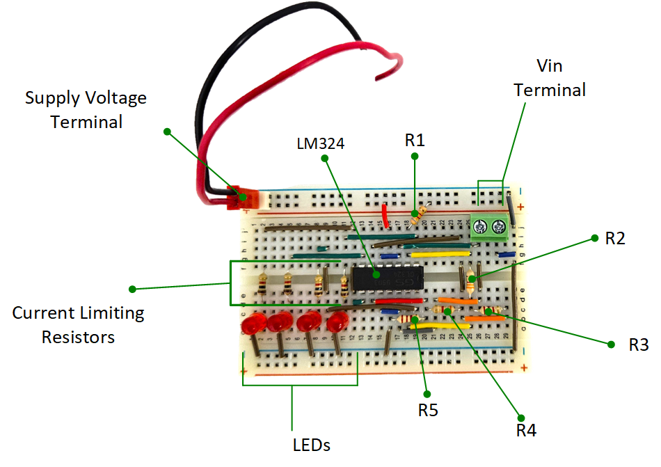
The purpose of breadboarding is to provide an actual simulation and real-time testing of the circuit. Verifying and testing the circuit’s operation also ensures all components work properly before final fabrication.
Testing and Prototyping Steps
- All the electronic components needed for the circuit design are collected. This includes jumper wires, a power supply or battery, and terminal blocks.
- The components are strategically placed for better observation of the circuit’s behavior. The LEDs are placed to resemble a “bar graph”.
- Jumper wires are utilized to facilitate connections between components.
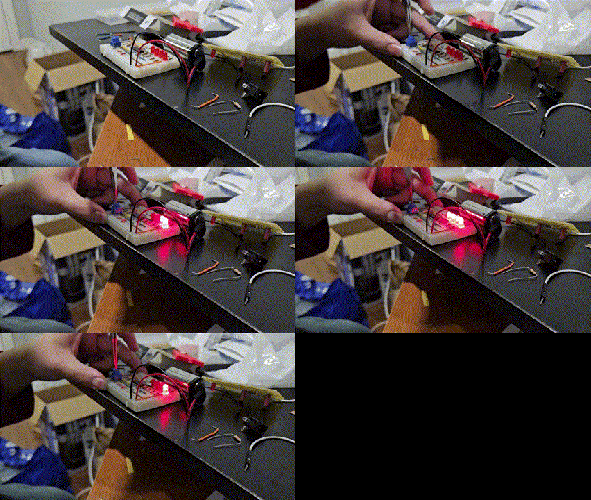
- The circuit’s functionality is tested by applying power (Vcc) and the necessary input parameters (Vin).
Simulation Expectation
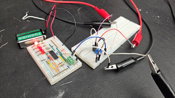
The circuit and the LM324 IC are both powered by a 9V battery. The battery is also connected to the series combination of R1 – R5 and the inverting input terminals of each opamp. The Vin terminal receives an input voltage that ranges from 0V to 6V. Each opamp compares this voltage with its corresponding reference voltage and should only turn ON the LED when the two are equal.
However, the LEDs turned ON with these parameters:
| Ref. Voltages | Measured Input Voltages | Voltage Difference |
| V1 = 5.31V | Vin1 = 4.8V | 0.51 V |
| V2 = 3.825V | Vin2 = 3.4V | 0.425 V |
| V3 = 2.835V | Vin3 = 2.6V | 0.235 V |
| V4 = 1.08V | Vin4 = 1.0V | 0.08 V |
The input voltages are a little off from the expected values. Additionally, there are some fluctuations introduced by Vin that affect the behavior of the circuit.
However, note that the actual values of resistors and actual reference voltages were not measured and included in the circuit analysis before. Each resistor has a tolerance of ±5% which may have a significant effect on the circuit’s operation.
Normally, in more complex circuits, tolerance analysis is included to determine the circuit design margin and provide some calculations for deciding and justifying the allowable amount of discrepancy between the expected and acquired parameters (Sachs, 2020). However, in this experiment, it’s decided to not go over this lengthy process. Instead, it’s recommended to just obtain actual reference voltage measurements using a multimeter and take it from there.
While it’s normal to obtain values with some inconsistencies in the actual simulation process, it’s still a great practice to implement solutions to reduce these discrepancies as much as possible.
Suggested Solutions
- Proper connections should be checked, and components should be properly inserted.
- Use a decoupling capacitor in the input voltage (Vin) to stabilize the voltage that goes in.
- Try experimenting with resistors that have different properties or use resistors with a lower tolerance.
- Try using a stable, regulated power supply instead of a battery.
If applying all these solutions didn’t make any improvement, then a more thorough circuit analysis might be needed. This includes understanding the operation of a comparator opamp and determining the practical limitations on the actual voltage range of the op-amp device being used (Electronics Tutorials, n.d.). But in this case, there’s no need to go over it thoroughly. Moreover, while breadboards are designed for prototyping, their limitations and disadvantages should also be acknowledged (Analog Devices, 2009).
PCB Design Layout (Autodesk Eagle)
For this project, through-hole components will be utilized in a single-layer board layout. This means that all traces must be on the bottom layer of the PCB. Designing a single-layer PCB may seem daunting at first, but with practice, it becomes easier.
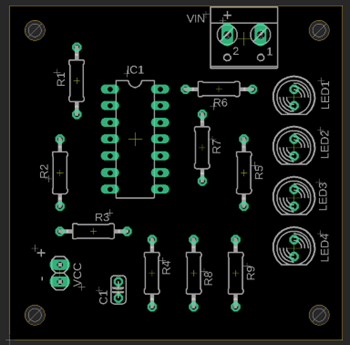
Components Placement
PCB Board Layout/Traces
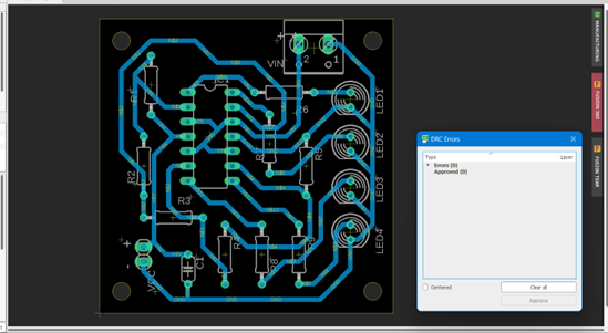
- Board Dimension: Height = 2 inches; Width = 2 inches
- Wire Width: 32 mills
Note that design rule checks (DRC) and electrical rule checks (ERC) are performed to ensure that there are no errors or violations in the circuit design. Design rules can be adjusted depending on the manufacturer’s requirements and capability.
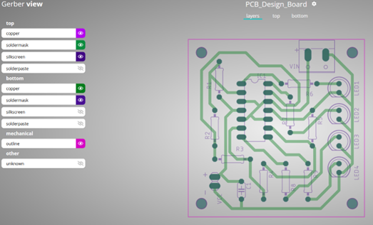
PCBWAY Gerber Viewer
PCB Fabrication
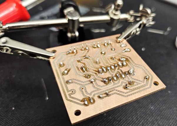
Normally, the Gerber files, extracted from Eagle software, can be forwarded to a PCB manufacturer or “PCB house.” These files encompass critical details such as copper layers, solder masks, silkscreen, and other important design features. For this project, the school’s in-house manufacturing facility undertakes the PCB fabrication process.
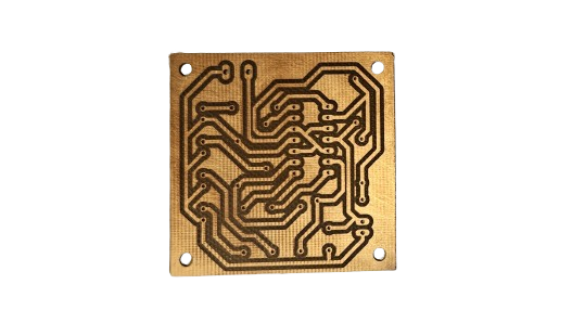
The problem, however, is some important details are left out, such as the solder mask and top silkscreen which indicates the proper orientation of the components. This is not a problem if the person who will solder the component knows every detail of the circuit’s PCB design.
But overall, in this project, the functionality is more important. To be fair, the board still looks professional and good for building permanent prototypes. Therefore, it’s decided to continue with the soldering process with the obtained fabricated board.
Recommended PCB Manufacturing Companies
When choosing a PCB manufacturing company, it’s essential to keep factors like cost, lead time, quality, and special requirements in mind. Here are some recommended companies that produce professional-looking PCB boards.
- JLC PCB
- PCBWAY
PCB Soldering
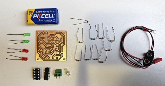
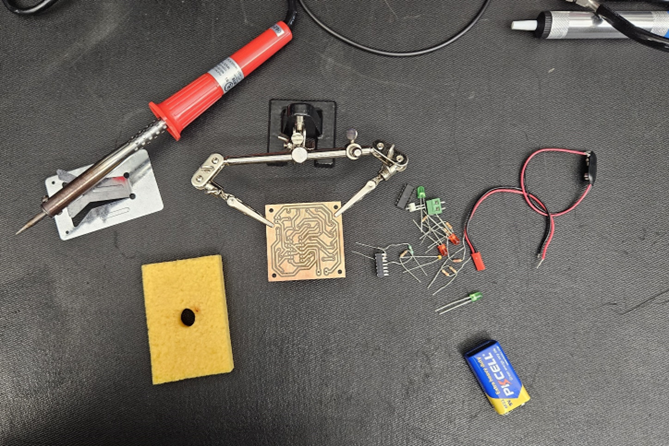
Tip: A “helping hand” tool is a great tool that holds the board and makes the soldering process more comfortable.
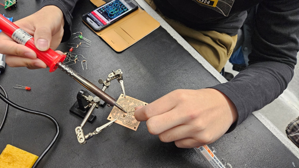
Final PCB Board
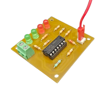
After soldering all the components, a final visual inspection is conducted to check for component orientation, cold solder joints, and insufficient solder. Additionally, a continuity test is performed on every trace in the circuit to check if there is a complete electrical path between two points. A continuity test helps ensure that there are no unintended connections (shorts) or open circuits in the soldered connections.
Bill of Materials
| Quantity | Device | Description | Part Name | Price |
| 1 | LM324N | IC OPAMP GP 4 CIRCUIT 14DIP | IC | $1.95 |
| 1 | R-US_0207/10 | RES 8.2KΩ 5% 1/4W | R1 | $1.95 |
| 1 | R-US_0207/10 | RES 3.3KΩ 5% 1/4W | R2 | |
| 1 | R-US_0207/10 | RES 2.2KΩ 5% 1/4W | R3 | |
| 1 | R-US_0207/10 | RES 3.9KΩ 5% 1/4W | R4 | |
| 1 | R-US_0207/10 | RES 2.4KΩ 5% 1/4W | R5 | |
| 4 | R-US_0207/10 | RES 1KΩ 5% 1/4W | R6, R7, R8, R9 | |
| 4 | LED5MM | LED RED DIFFUSED 5MM | LED1, LED2, LED3, LED4 | $1.95 |
| 1 | PINHD-1X2 | PINHEADER 2.54MM | VCC | |
| 1 | W237-02P | TERM BLK 2P SIDE ENT 5.08MM | VIN | $1.32 |
| 1 | C-US050-024X044 | CERAMIC CAP 10UF | C1 | $1.95 |
Discussion of Results
This project has provided us with a detailed understanding of the operation of comparators in electronic circuits. Most importantly, it has allowed us to gain knowledge and proficiency in utilizing various software programs to simulate electronic circuits and create intricate printed circuit board (PCB) designs.
In addition, this project highlighted the crucial role of practical experience and experimentation in circuit design and implementation. For instance, we have learned that it is crucial to assemble the circuit in the breadboard initially and test it to ensure its proper functioning before proceeding to soldering and final fabrication.
The overall project was an invaluable learning experience for us. We gained insights into the behavior of electronic components in real-world scenarios.
References
MT-100: Breadboarding and prototyping techniques – analog … (n.d.). https://www.analog.com/media/en/training-seminars/tutorials/MT-100.pdf
Storr, W. (2022a, August 2). Op-amp comparator and the op-amp comparator circuit. Basic Electronics Tutorials. https://www.electronics-tutorials.ws/opamp/op-amp-comparator.html
Sachs, J. (n.d.). Tolerance analysis. EmbeddedRelated.com | Embedded Systems. https://www.embeddedrelated.com/showarticle/1353.php
Creator and Editor at AnitoCircuits.com based in Toronto