I made this project as an Electronics Engineering Technician (EEN) student in my digital electronics course. I enjoyed working on it and learned a lot of things. Here, I provided an overview of how I made this simple yet fascinating project.
Design Goals
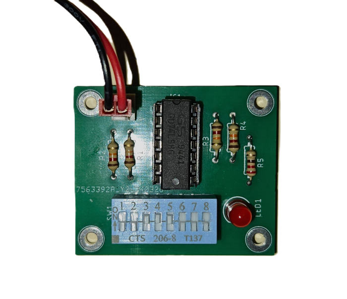
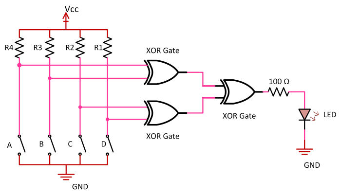
The given diagram shows a parity checker circuit that implements XOR (exclusive OR) gates. The project aims to design the PCB board of the circuit on EAGLE and build it physically. This includes simulating the circuit on ORCAD and verifying its working principle. It’s also expected to generate the truth table and represent the circuit in a Boolean expression.
| Parameters | Value | |
| Operating Voltage | 5 V | |
| Output Voltage | 3.4 V | |
| Input Logic Voltage | LOW | HIGH |
| 0 V | 5 V | |
| Switch pin config. | 4, 5, 6 & 7 | |
| IC gates pin config. | XOR 1 | 1, 2 & 3 |
| XOR 2 | 4, 5 & 6 | |
| XOR 3 | 11, 12 & 13 | |
Project Description
Parity checkers, in general, are circuits that receive a data sequence and checks whether any error is present in that data. The given circuit though is an Even Parity Checker that uses Exclusive-OR (XOR) gates to perform the parity check operation. An XOR gate is a digital logic gate that outputs high only when one input is high. In this project, three XOR gates are employed to compare a sequence of input bits and produce the expected output.
Switch Configuration
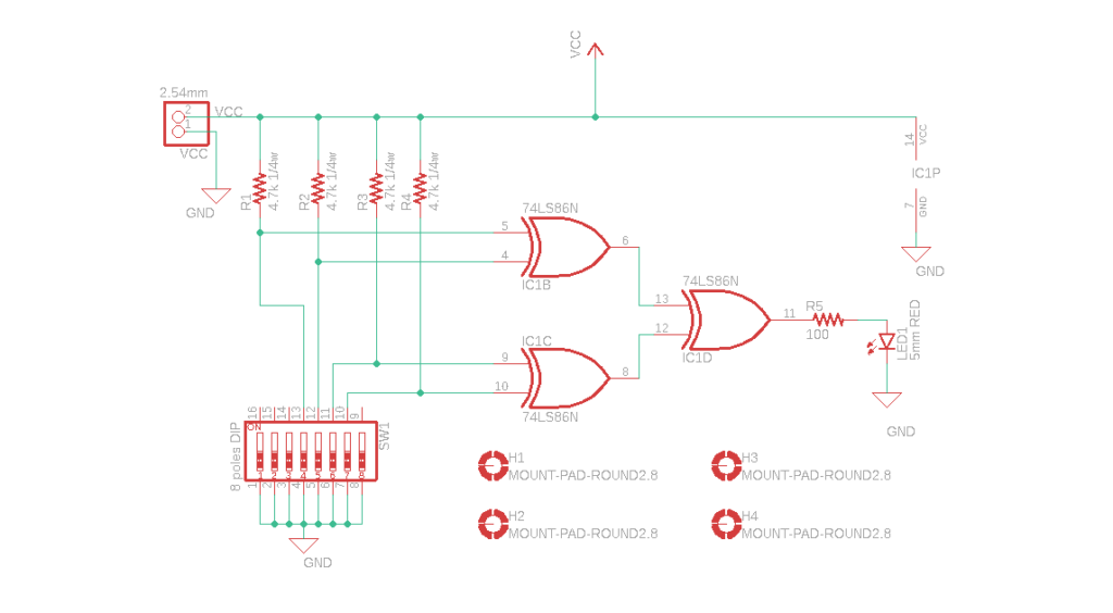
Switches are parameters included to act as the four binary data by controlling the states of the inputs. The switches are configured in active low connections (see figure 2), meaning when the switch is closed, the input pin connected to it receives a low voltage (VL), “logic 0.” The input pin is shorted to ground; therefore, it will not get a high signal.
When the switch is open, the input pin receives a high voltage (VH), “logic 1.” This happens because the pin is connected to a pull-up resistor, which gets a stable high signal from the supply voltage.
Pull-up Resistors
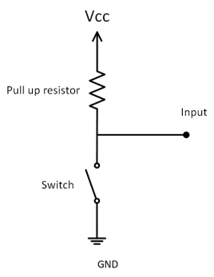
10k ohm pull-up resistors are used to draw enough input current of around 0.5 mA at a nominal input voltage of 5V. The ideal resistance is calculated using the following formula:
\[ R=\frac{V_{IH}}{I_{IH}}=\frac{5V}{0.5mA}=10kΩ \]
Additionally, note that these input parameters are within the allowed range based on the data sheet of the IC being used. However, while any resistance value can be used, note that the current-sinking and sourcing ability of each input pin, in addition to the operating voltage, limits the functionality of digital logic gates. It is therefore important to identify the maximum resistance and consider it while making decisions.
\[R_{max}=\frac{V_{CC}-V_{IH\left(min\right)}}{I_{IH}}\]
Featured Logic Gates IC
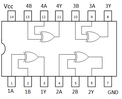
The circuit utilizes the 74LS86 IC, comprising four independent 2-input Exclusive-OR gates. This IC can function with supply voltages ranging from 4.75V to 5.25V.
| GD54/ 74LS86 | |
| Vcc | 4.75V to 5.25V |
| Output Voltage | 2.5V to 3.4V |
| Current – Output High, Low | 400µA, 8mA |
| Input Logic Level – Low | 0.8V |
| Input Logic Level – High | 2V (min) |
| Number of Circuits | 4 |
| Number of Inputs | 2 |
| Datasheet: https://datasheetspdf.com/pdf-file/567162/ETC/GD74LS86/1 | |
74LS86 Pin Outs Diagram
This project is also designed to follow specific gate pin configurations, based on the above parameters. It’s expected to use pins (1, 2 & 3) as XOR1, pins (8, 9 & 10) as XOR2, and pins (11, 12 & 13) as XOR3.
Design Simulation
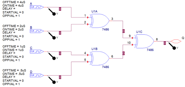
There are several better software programs to simulate digital circuits. But this time, OrCAD/PSpice is employed to verify the functionality of the given circuit by producing a transient response.
OrCAD Schematic Capture
Transient Simulation Result
The vertical regions, as shown in the figure below, are the 16 combinations generated from the 4-bit input (A, B, C & D). Note that an input signal (Digiclock) produces data sequence per time which also generates the output data sequence of the circuit (Q). This is just the best way to simulate logic gates in OrCAD.

Truth Table
The truth table for the circuit can be generated by analyzing the circuit itself or observing its transient response (see Figure 5). But to determine whether a given data has even or odd parity, a simple principle can be applied: the sum (without carries) of an even number of 1s is always 0, while the sum of an odd number of 1s is always 1. Thus, adding up all the bits in the code will reveal its parity.
The truth table below confirms that the output of the circuit is 1 only when the four input bits have an odd number of 1s. Conversely, the output is 0 when the input bits have an even number of 1s. Based on this analysis, it can be further concluded that the circuit is an Even Parity Checker.
| A | B | C | D | OUTPUT |
| 0 | 0 | 0 | 0 | 0 |
| 0 | 0 | 0 | 1 | 1 |
| 0 | 0 | 1 | 0 | 1 |
| 0 | 0 | 1 | 1 | 0 |
| 0 | 1 | 0 | 0 | 1 |
| 0 | 1 | 0 | 1 | 0 |
| 0 | 1 | 1 | 0 | 0 |
| 0 | 1 | 1 | 1 | 1 |
| 1 | 0 | 0 | 0 | 1 |
| 1 | 0 | 0 | 1 | 0 |
| 1 | 0 | 1 | 0 | 0 |
| 1 | 0 | 1 | 1 | 1 |
| 1 | 1 | 0 | 0 | 0 |
| 1 | 1 | 0 | 1 | 1 |
| 1 | 1 | 1 | 0 | 1 |
| 1 | 1 | 1 | 1 | 0 |
Boolean Expression
The circuit is represented by a Boolean expression using the sum of product terms (SOP), thus verifying the implementation of XOR logic gates.
PCB Design (Autodesk Eagle)
There are several software programs available for designing printed circuit boards, both free and paid, which can be used from prototyping to industrialization. Eagle is a recommended software but comes with a significant cost. However, what I like about it is that it comes with an extensive component library to start with.
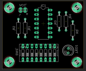
Moving on, this design process expects the use of through-hole components on a single-sided PCB layout with a maximum board dimension of 2 x 3 inches. Also, please note that a terminal block or pin header is included as an input terminal for the power supply. For the switches, an 8-pole DIP switch is used with specific pin configurations defined by the given parameters.
Eagle Schematic Capture
Component Placement
PCB Layout/ Traces
Board Dimension: Height = 1.5 inches ; Width = 1.8 inches
Wire Width: 32 mills
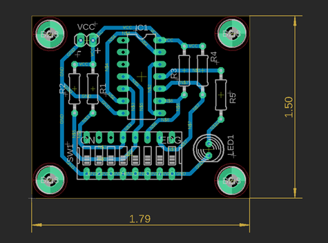
Design rule checks (DRC) and electrical rule checks (ERC) are performed to ensure there are no errors or violations in the PCB design.
PCB Fabrication
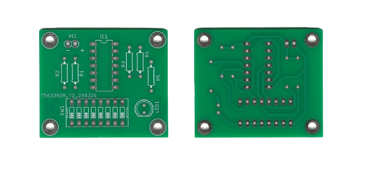
The Gerber files, which contain crucial information such as copper layers, solder masks, silkscreen, and other important design features, can be extracted from Eagle software. These files can then be sent to a PCB manufacturer or “PCB house” to produce the circuit board. In this project, we have chosen to utilize JLCPCB for the manufacturing of our circuit board.
Soldering
Soldering is the process of creating secure electrical connections between components on a printed circuit board. In this step, accurate placement of components and good solder joints are ensured for the circuit to work properly.
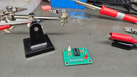
While soldering is a fundamental skill for anyone working with electronics. It’s important to remember that practice makes perfect. As we gain experience, our soldering skills will improve and will result in reliable and professional-looking circuits.
Final Fabricated Circuit Board
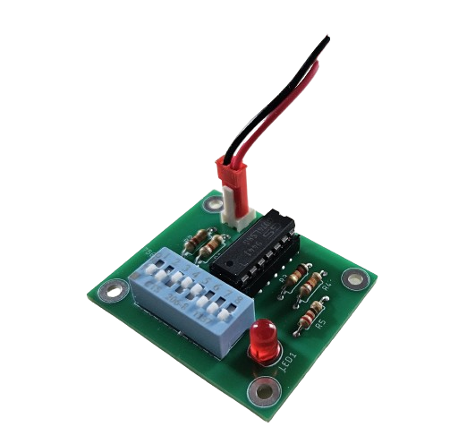
Before testing the circuit, a final visual inspection must be conducted on the entire board for any missed connections, cold solder joints, or defects. It’s important to check the continuity and resistance of every trace to ensure that there is a complete path for the current to flow. Lastly, clean the board with isopropyl alcohol to remove the flux residue.
Bill of Materials
| Quantity | Device | Description | Price |
| 1 | 74LS86N | QUAD 2-INPUT EXCLUSIVE-OR (XOR) GATE | $0.975 |
| 4 | R1, R2, R3, R4 | RES 10KΩ 1/4W | $0.975 |
| 1 | R5 | RES 100 Ω 1/4W | |
| 1 | LED5MM | RED LED 5MM | $0.15 |
| 1 | SW_DIP-8 | DIP SWITCH 8 POLES | $3.69 |
| 1 | PINHD-1X2 | PIN HEADER 2.54MM | $0.15 |
| 1 | IC SOCKET | 14DIP IC SOCKET | $2.59 |
Discussion of Results
The parity checker circuit is a practical example of using combinational logic gates as an error detection system. The circuit turns on the LED only when it detects an error, which occurs when the input bits have an odd number of 1s. Simultaneously, the LED remains off when there is no error detected from the data, which happens when the input bits have an even number of 1s. This type of circuit is mostly employed in digital communication systems as a common error-detection method to ensure data integrity.
Along the way, the design and simulation of the circuit using computer-aided software programs, with the physical assembly and testing confirm its operation and functionality. This project not only shows how logic gates or digital electronics work but also highlights the significance of practical or hands-on experience and experiments in circuit design and analysis.
In summary, this project serves as a valuable educational resource, offering valuable insights into electronic design and the behavior of electronic components in practical, real-world scenarios.
References
Pull-up resistors. Pull-up Resistors – SparkFun Learn. (n.d.). https://learn.sparkfun.com/tutorials/pull-up-resistors/all
Teja, R. (2021, July 2). Parity generator and parity check. ElectronicsHub USA. https://www.electronicshub.org/parity-generator-and-parity-check/
GD74LS86 Datasheet link. https://datasheetspdf.com/pdf-file/567162/ETC/GD74LS86/1
Download pdf file
Creator and Editor at AnitoCircuits.com based in Toronto