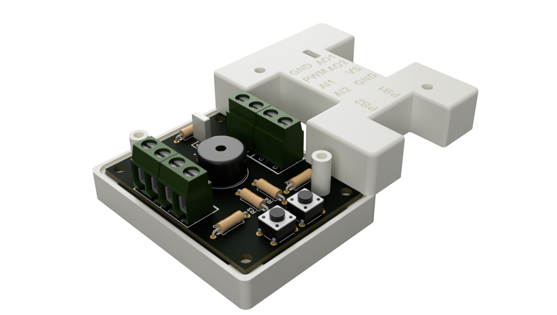
Description
LabJack is a device that provides analog inputs/outputs, digital inputs/outputs, and more that you can use in a computer-based instrumentation and control system. For example, suppose you want to create a computer-based project that collects data from various sensors and controls different outputs, you can use a LabJack to interface between the computer and the inputs and outputs.
However, LabJack devices do not typically include built-in components like switches, LEDs, or actuators. Instead, they just provide the interfaces to connect these external components to a computer-based system.
So in this project, we’re going to build a board device composed of some of these basic electronic components that we can use for testing the LabJack ports’ functions.
Getting Started
The main objective of this project is to design this I/O board for LabJack with a CAD software application. And from the generated CAM/CAD files, we should be able to manufacture the parts and physically build the project. I will also walk you through the process of how I did it.
The circuit design is already provided (see figure below), so I will begin by designing the PCB and creating an enclosure.
Part 1: Schematic Capture
This circuit consists of only a few electronic components; so, it’s not that complicated for me to understand and draw it in the workspace.
However, the most “not so exciting part” of this process is finding the component you need with the right footprint and 3D model. Well, I want to make sure that the component comes with the complete package because I want to see how it will look in 3D at the end.
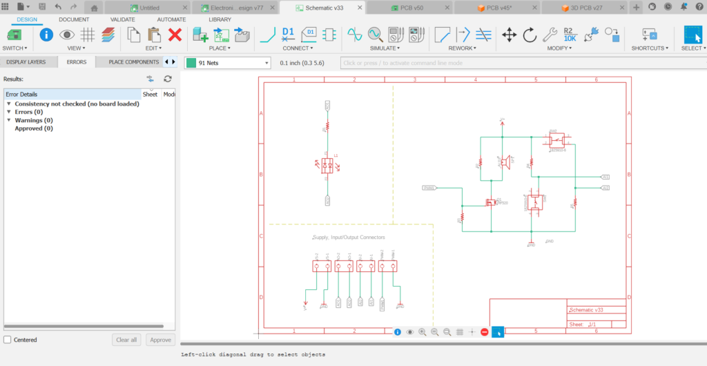
I used the component library in Fusion 360 to find and place components on the schematic. Of course, certain parts were not available, so I had to create custom components by defining their parameters. This is where the datasheet comes in handy.
ⓘ Note
If you can’t create a custom component in Fusion, try finding it from websites like UltraLibrarian.com or SnapEDA.com.
Part 2: PCB Design
With the schematic above, we can now proceed to design the circuit board. However, before we continue, it’s important to have a clear understanding of what the circuit is supposed to achieve. This will help with the component placement.
Well, in this simple project, we can overlook factors like signal integrity and thermal management, but we should at least consider how our PCB will look or if we can assemble it easily. So, I tried to place certain components in specific and strategic locations. I really want to make my PCB look organized and appealing.
Anyways. Moving on. I defined the physical dimensions and shape of the PCB according to the project requirements. However, when designing PCBs, I always try to set the board outline depending on the number of components. I mean it’s a skill if you can fit a lot of components into a limited board outline while ensuring its functionality, reliability, and manufacturability.
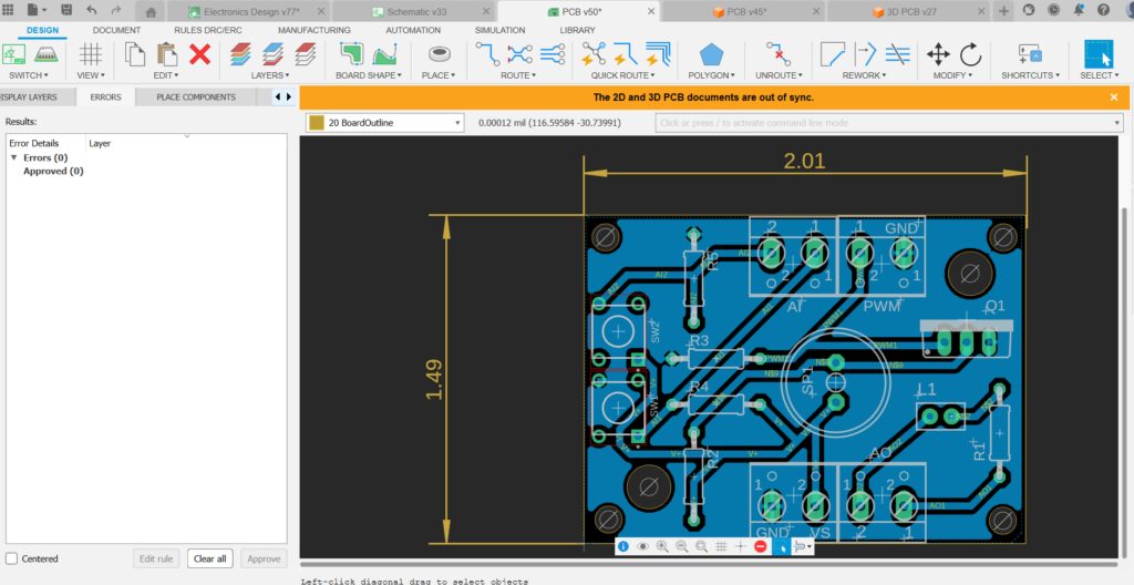
Here, the board dimension is 1.5 x 2 inches. I also used a width of 32 mills for all of the traces. Additionally, I added a copper pour on the ground layer to create a solid ground plane. This helps in reducing noise and improving overall performance.
Another note: This project was actually created as part of my course requirements, and I’m only allowed to design a single-layer board layout. So, that’s why I’m only utilizing the bottom layer as shown in the figure below.
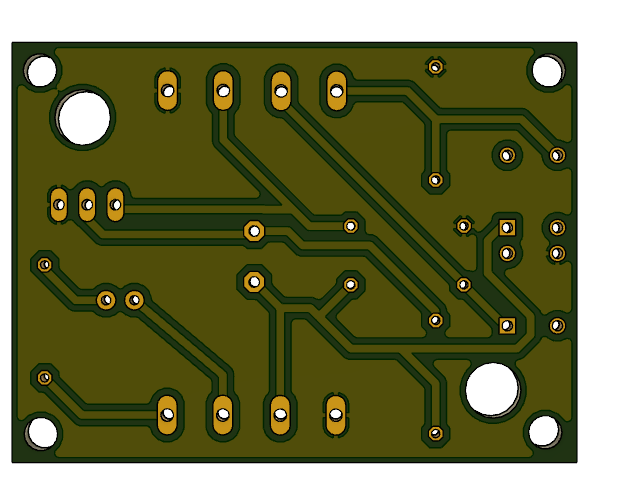
I include mounting holes and cutouts for the PCB because I want it to fit securely into its enclosure. What I like about Fusion is that I can always go back and forth to adjust the board outline.
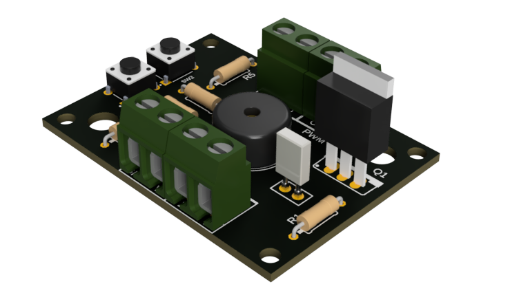
Rendered 3D PCB
After finalizing the PCB design, let’s see how its rendered 3D model looks like. I just want to visualize the final product and check for any potential issues. In my opinion, this also presents the design in a professional manner.
Part 3: PCB Enclosure
I then modelled an enclosure for the PCB. Creating 3D models wasn’t something I’m used to but I’m really starting to enjoy and love it.
Instead of starting with a basic sketch of the enclosure outline from scratch, I imported the PCB model into the Fusion 360 workspace. From there, I defined and offset planes and made projections to project the board outline and screw hole positions of the PCB. After that, I added some clearance and used the extrude feature and other tools to complete the model. I believe there are many ways of doing it but I can’t think of any easy way to create the enclosure outline.
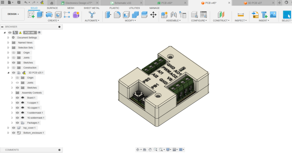
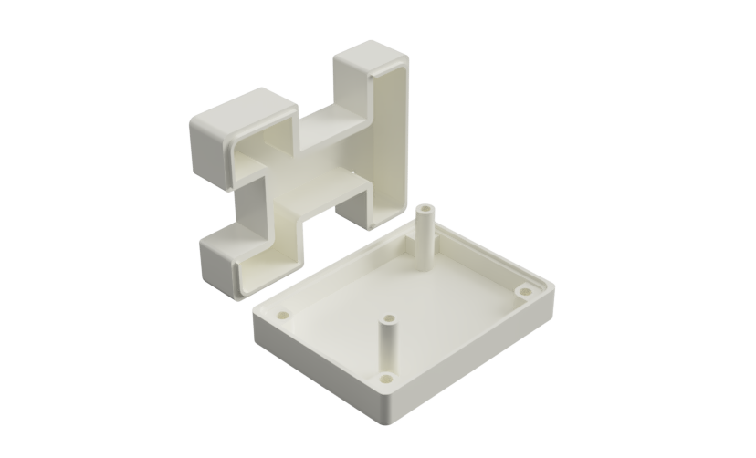
Please take note that I have divided my enclosure into two parts: the base and the lid or cover. I initially wanted to make it a snap-fit feature, but I decided to use screws instead. You can see the mounting holes on the top cover.
So, after countless hours of designing and iterating my model, I was finally able to create a decent-looking enclosure design for my PCB. Now, all I need to do is to 3D print it.
Final Project Assembly
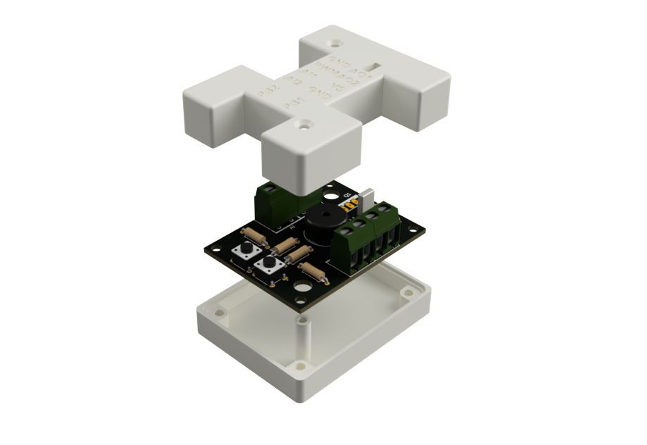
Moving on, here’s how the final rendered project assembly looks like. There should be two screws on top, but never mind. I think you get the idea of how the project is assembled.
After finalizing the design, I prepared it for manufacturing by exporting the parts (base and lid) as STL files. These files contain the detailed 3D model of my enclosure. You can also use formats like OBJ and 3MF but I think they’re better suited for more complex and detailed prints. Aside from that, I prefer STL files because they are universally supported by nearly all 3D printers and slicing software.
I initially planned to slice and print this enclosure myself with my school’s 3D printer, but I decided to send it to a manufacturer instead. Since I use JLCPCB for most of my PCB fabrications, it might be best to let them print the enclosure as well.
ⓘ Note
If you want to download the Gerber files of the PCB and STL files of the enclosure, I uploaded all the files of this project to my GitHub repository
This is how my actual project looks like. There are still some areas of improvement but I’m satisfied with the end result. It also works when I tested it with the LabJack.
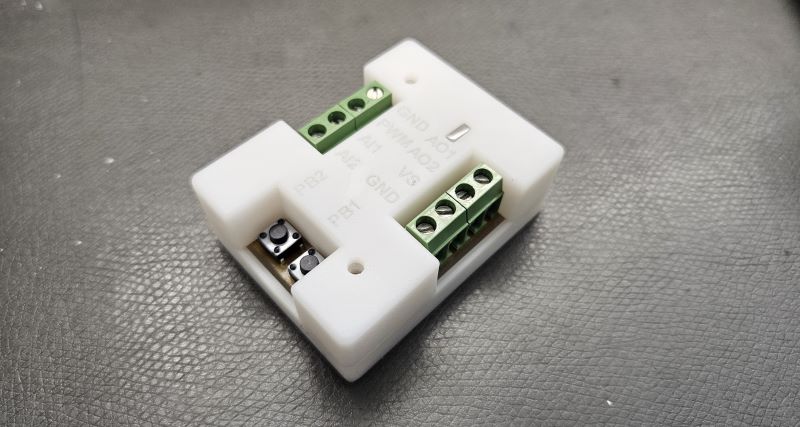
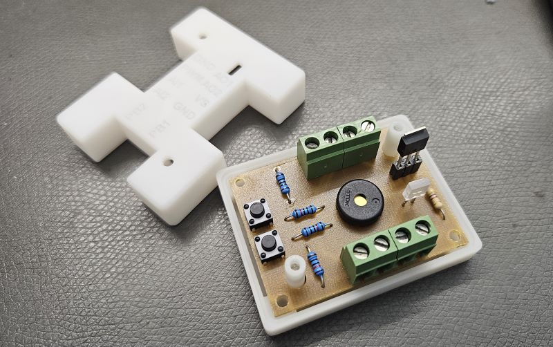
Project Application
From the given circuit below, we will not read from sensors but rather just from simple push buttons. From there, we can control a bi-directional LED and a buzzer. That’s it!
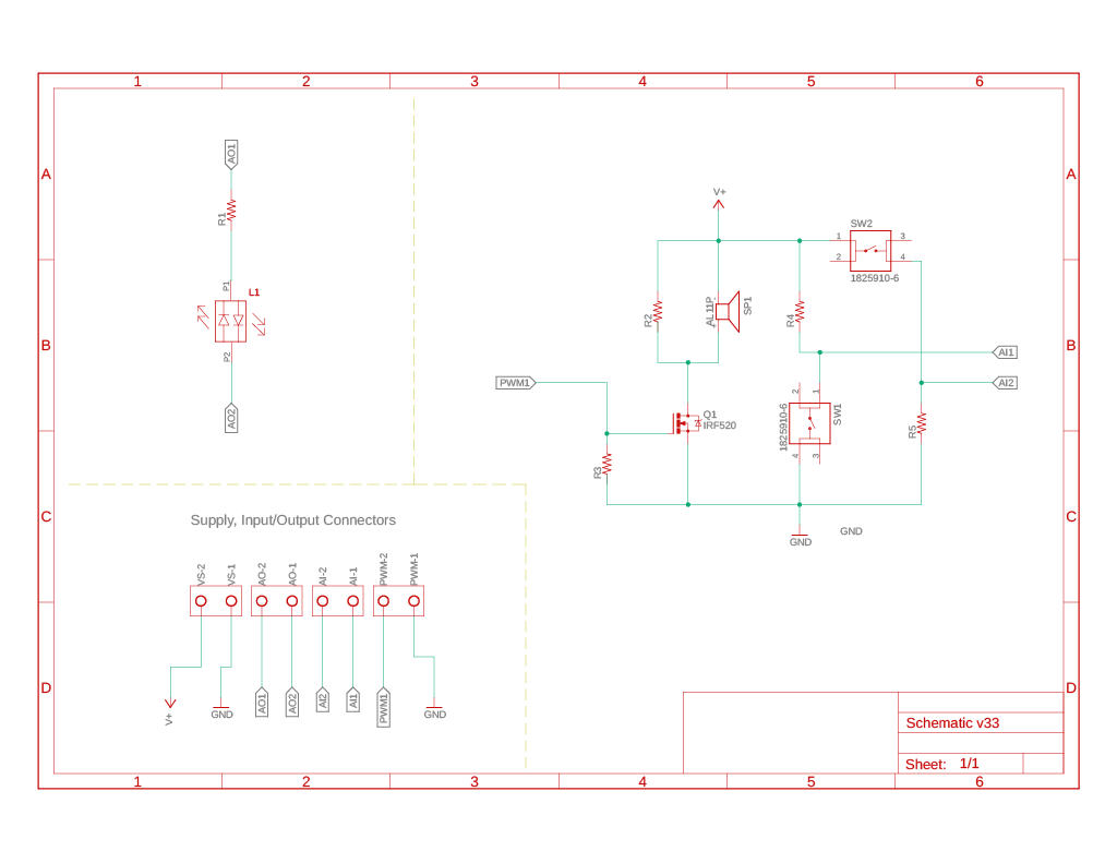
The bi-directional LED serves as an output and the specific color will turn ON depending on the potential difference across its terminals. The buzzer will produce a noise or pitch when a PWM signal is active. Also, please note that an N-channel MOSFET is included to drive the buzzer. On the other hand, switches act as inputs and will provide either 0 or 5 volts to the LackJack.
Here, we can see that the circuit is mainly for testing the functionality and ports of the LabJack by integrating switches, LEDs, and a buzzer.
In addition, the figure below shows a block diagram of how the I/O Device is connected to the LabJack. Please take note of the ports as these ports are typically labeled according to their function.
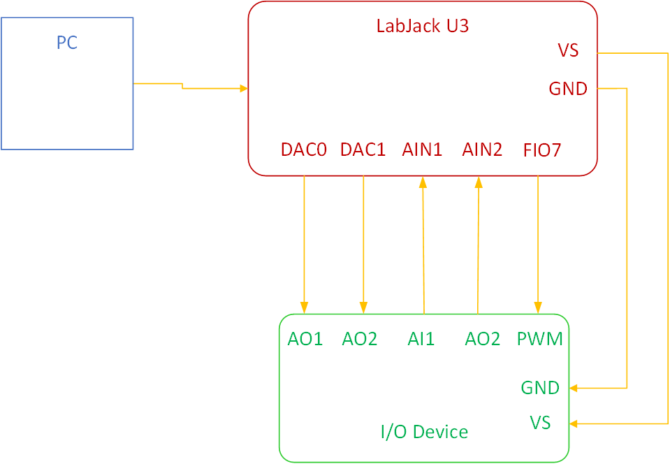
Note:
AO1andAO2must be connected toDACports of the LabJack.- We can connect the AI ports of the board to any
AINports of the LabJack we like. - Similarly, we can use any
FIOports for thePWM.
Creator and Editor at AnitoCircuits.com based in Toronto